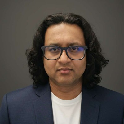
About Me
I am a materials scientist at the University of Bristol. My research centres on electron microscopy and the synthesis of 2D materials, with a particular interest in watching materials form in real time inside the electron microscope. I have spent the last 12 years working across Nepal, Japan, and the UK, studying nanoscale reactions as they happen and developing scalable routes to graphene and related materials.
Core Research Interests
🔬 In Situ TEM and Metal-Carbon Dynamics
I specialise in visualising nanoscale reactions as they happen, using in situ heating and electrical biasing inside the TEM. Over 12 years I have systematically studied the interaction of ten different metals with amorphous carbon under applied bias voltage, directly observing real-time graphitisation, electromigration, catalytic nanotube growth, and nano-soldering of carbon nanostructures.
- Ten metal systems studied individually (Fe, Ni, Cu, Mo, Sn, In, Ga, Co, Pd, CuNi alloy), with first-author or corresponding-author publications on each.
- Techniques: HRTEM, HAADF-STEM, EELS, EDX, SAED, cryo-TEM, EFTEM, operando heating and biasing holders.
- Instruments: JEOL JEM ARM 200F, JEOL 2100, FEI Osiris, FEI Tecnai.
⚛ 2D Materials Synthesis and Waste-to-Graphene CVD
Extensive experience in scalable growth of 2D materials, from wafer-scale CVD at the Cambridge Graphene Centre to pioneering waste-derived graphene conversion.
- Wafer-scale (200 mm) CVD synthesis and transfer of graphene, hBN, MoS2, and WS2 within the EU Graphene Flagship. Commissioned an AIXTRON MOCVD reactor for pilot-scale growth.
- Pioneered waste-to-graphene CVD from solid waste plastic (Carbon 2014, 200+ citations), extended to waste chicken fat, camphor, tangerine peel oil, and waste latex.
- Demonstrated graphene synthesis at record low temperatures: 150°C (In catalyst) and 180°C (Sn catalyst).
- Co-authored rapid microwave plasma CVD enabling graphene growth in under 40 seconds at below 600°C.
💻 Computational Tools for Microscopy and Synthesis
Alongside experimental work, I develop software tools that support day-to-day microscopy and synthesis planning.
- Automated SAED phase identification software and validated XRD/SAED diffraction simulators.
- Literature-mining and cross-referencing tools to help prioritise synthesis targets, with automated thermodynamic due diligence.
- Machine Learning Certification, DeepLearning.AI (Credential ID: 9G6WGJ2R9D3N).
Professional Experience
Electron Microscopy Specialist
University of Bristol | Jul 2024 - Present
- Design and conduct independent operando TEM experiments (heating and biasing holders) to observe growth, transformation, and property evolution at the nanoscale across the Faculty of Science.
- Manage and maintain a suite of JEOL electron microscopes within the Chemical Imaging Facility, supporting research across the School of Chemistry and beyond.
- Developed automated SAED phase identification software and validated XRD/SAED simulators to support facility users.
- Design and deliver structured TEM training programmes; assess researcher competence through practical examination.
R&D Engineer / Materials Process Engineer
Advanced Furnace Technology, Cambridge | Dec 2023 - Jun 2024
- Led process development for large-scale tantalum carbide (TaC) growth for high-temperature applications.
- Contributed to furnace design and specification for industrial scale-up: repeatability, throughput, safety, and practical manufacturability.
Postdoctoral Research Associate
University of Cambridge (Cambridge Graphene Centre) | Dec 2019 - Nov 2023
- Led EU Graphene Flagship work packages, coordinating experimental activities across 14+ researchers at multiple European institutions, managing milestone delivery and EU reporting.
- Developed 200 mm wafer-scale CVD synthesis and transfer of graphene, hBN, and TMDCs. Commissioned AIXTRON MOCVD reactor for pilot-scale 2D material growth.
- Supervised PhD students through experimental design, data analysis, and publication preparation.
- Contributed to TEM studies of graphene-based battery materials and terahertz photodetector heterostructures.
Postdoctoral Researcher / Nanotechnology Platform Engineer
Nagoya Institute of Technology | Apr 2015 - Nov 2019
- In situ TEM studies of ten metal-carbon systems (Fe, Ni, Cu, Mo, Sn, In, Ga, Co, Pd, CuNi) under applied bias voltage: directly observed graphitisation, electromigration, catalytic nanotube growth, and nano-soldering. Published on each system individually.
- Demonstrated graphene synthesis at record low temperatures: 150°C (In catalyst), 180°C (Sn catalyst).
- Extended waste-to-graphene CVD to waste chicken fat, camphor, tangerine peel oil, and waste latex.
- Co-authored rapid microwave plasma CVD: graphene growth in under 40 seconds at below 600°C.
- Mentored undergraduate and graduate students; several published first-author papers under my guidance.
- Awarded Certified Senior Engineer, Nanotechnology Platform Japan (MEXT, 2019).
Education and Certifications
PhD in Engineering
Nagoya Institute of Technology | 2012 - 2015
- Thesis: Synthesis of graphene and hexagonal boron nitride using solid precursors by chemical vapour deposition. Advisor: Prof. Masaki Tanemura.
Master of Engineering
Chubu University | 2012
- Focused on plasma physics, production of TiN/TiO2 films, and their properties.
BSc in Physics
Tribhuvan University | 2008
Machine Learning Certification
DeepLearning.AI | Credential ID: 9G6WGJ2R9D3N
Research Impact
- Publications: 50+ peer-reviewed outputs, h-index 19, i10-index 28, over 1,000 citations.
- Pioneering work: First demonstration of waste plastic to graphene via CVD (Carbon 2014, 200+ citations). Record low-temperature graphene synthesis (150°C).
- Advanced Microscopy: Expert in (S)TEM, EELS, EDX, SAED, cryo-TEM, EFTEM, and operando heating/biasing experiments.
- Instrumentation: JEOL JEM ARM 200F, JEOL 2100, FEI Osiris, FEI Tecnai, AIXTRON MOCVD, CVD systems.
- Software tools: Automated SAED phase identification and validated diffraction simulators in routine use.
- Peer review: Active reviewer for Nano Letters, Nanoscale, Carbon, ACS Applied Materials and Interfaces. Multiple Outstanding Reviewer awards.